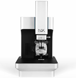
Park NX10, a versatile and high performing research tool, providing excellent AFM capabilities in nanofabrication and -manipulation and the ability to image and analyze many diverse nano materials
Park has continually added AFM design features to match the pace of nanotechnology innovation, for instance, our AFM can easily observe and comprehend nanostructures in biomaterials at the cellular level such as organelles and even DNA and RNA.
SANTA CLARA, Calif. (PRWEB)
March 02, 2020
Visit the Park Systems at Booth 2436 at Pittcon and find out more about their latest innovations in AFM technology
Park Systems, a leader in Atomic Force Microscopy (AFM) since 1997 is exhibiting at Pittcon March 1-5 at the McCormick Place Convention Center in Chicago IL. At this year’s Pittcon, Park Systems will showcase their complete line of innovative AFM products including the industry’s leading AFM product, Park NX10, known for its nanoscale accuracy and ease of use that allows innovative research. Park also features Park XE7, the scientific industry’s most affordable, research-grade AFM with innovative design features, providing AFM researchers with a cost-effective solution that doesn’t compromise quality or functionality.
“Pittcon offers us an excellent opportunity to showcase our unique set of AFM technologies with advanced nanoscale imaging,” comments Keibock Lee, President Park Systems. “Park has continually added AFM design features to match the pace of nanotechnology innovation, for instance, our AFM can easily observe and comprehend nanostructures in biomaterials at the cellular level such as organelles and even DNA and RNA.”
Park NX10 is a versatile and high performing research tool, providing researchers excellent AFM capabilities in nanofabrication and -manipulation and the ability to image and analyze many diverse materials in nanomaterials research. Park NX10 offers dedicated software and various modes and options to enable other specialized applications such as nanopatterning, scratching, and even electrical field oxidation.
Park NX10 SICM provides life science researchers with both AFM and Scanning Ion Conductance Microscopy (SICM) techniques on the same Park NX10 system. SICM enables life scientists to image biomaterials in a liquid environment therefore allowing for the discovery of the true morphology of biomaterials in a totally non-invasive way. Characterizing electrical, magnetic, mechanical, and morphological properties of materials are possible with the dedicated operating modes available with Park AFM and this unique functional nanoscale tool also provides researchers excellent AFM capabilities in nanofabrication and -manipulation.
Park AFMs feature a comprehensive range of scanning modes including PinPoint™ conductive AFM for well defined electric contact between the tip and the sample, conductive probe AFM to simultaneously image topography and conductivity of the sample surface, electrostatic force microscopy, Kelvin probe force microscopy, and more. Patented by Park Systems, dynamic contact electrostatic force microscopy (DC-EFM) actively applies an AC voltage bias to the cantilever and detects the amplitude and the phase change of the cantilever modulation with respect to the applied bias.
Park’s reputation as the AFM technology leader is due to their superior AFM design which guarantees accurate, reliable, and reproducible results. “In every field – materials science, electronics, life science, nanotechnology, we keep up with the exhilarating pace of metrology innovations so scientists can focus on getting results,” adds Lee.
Whatever your nanometrology needs are for material research, Park AFM has the expertise in nano materials to get the results you need. Stop by our booth at Pittcon where we want to hear about your research and share our AFM solutions.
About Park Systems
Park Systems is a world-leading manufacturer of atomic force microscopy (AFM) systems with a complete range of products for researchers and industry engineers in the chemistry, materials, physics, life sciences, and semiconductor and data storage industries. Park’s AFM provides the highest data accuracy at nanoscale resolution, superior productivity, and the lowest operating cost, thanks to its unique technology and innovative engineering. Cutting-edge AFM automation and nanometrology solutions provided by Park’s team of 100% committed professionals improves workplace productivity. Park System Inc., headquartered in Santa Clara, CA has global manufacturing and R&D headquarters in Korea and is supported worldwide with regional headquarters in the US, Korea, Japan, Singapore, Germany, China and Mexico. Park Systems high-performance scientific instruments explore new scientific phenomena that enable scientists around the globe to contribute to impactful science that helps humanity grow and improve life standards.
Please visit http://www.parksystems.com or call 408-986-1110 for more information.
Share article on social media or email:

